PCB Design Services
Asia Pacific Circuits has the knowledge and tools to make the design of your PCB no matter how large or small. We provide a full range of PCB design services spanning the entire product life cycle. Asia Pacific Circuits use the industries top tier circuit board design tools and are driven to be the best.
Legend:
- Multilayer PCB Design
- RF PCB Design
- Flex PCB design
- High density PCB
- High-Speed PCB
Asia Pacific Circuits Also Provide Printed Circuit Board Design Services
Are you unsure of how to design the perfect prototype for your business? Or do you not know where to start from? Whatever your worry is, Asia Pacific Circuits is here to provide a complete range of prototype development services, from the concept to the manufacturing. Yes, we provide printed circuit board design services too. Provide us your concept and let us modify, design and manufacture it to suit your requirements.
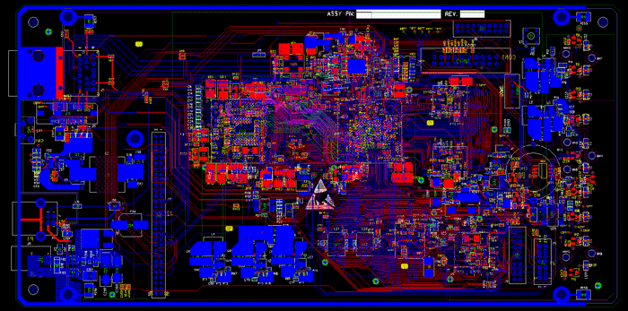
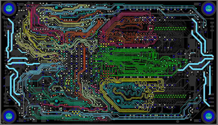
PCB Design Capability
- High speed, multilayer digital PCB designs(Bus routing, differential pairs, matched lengths).
- HDI PCB Designs with micro vias and advanced materials – Via-in-Pad, laser micro vias.
- Extensive RF and analog printed circuit board design experience (printed antennas, guard rings , RF shields…).
- PCB Layer management for signal integrity and impedance control.
- Signal integrity issues to meet your digital circuit board design needs (tuned traces, diff pairs…).
- High density SMT designs (BGA, uBGA, PCI, PCIE, CPCI…).
- DDR, DDR2, DDR3 and differential pair routing expertise.
- Flex PCB designs.
- Low level analog PCB designs for metering.
- Ultra low EMI designs for MRI applications.
- Complete assembly drawings.
- Drill, panel and cutout drawings designed.
- Professional fabrication documents created.
CAD Platforms
- Altium Designer
- Cadence Allegro
- PADS
- Orcad