PCB Manufacturing Capabilities

As a China PCB manufacturer for more than 17 years, we are very professional, not only in PCB fabrication but also in PCB assembly our advantages show as following:
1. Quotation for Conventional PCB within 2 hours, urgent offer within 1 hours.
2. Rich experiences in Conventional PCB manufacturing, professional suggestions from design stage in order to avoid anyimpracticable design.
3. Rich experience as PCB manufacturer enhances our understanding of oversea clients’ requests, especially requests from North America and European customers.
4. Different from other PCB manufacturer in China, we can accept sample order, small quality, series, as well as batch PCB fabrication, because we have 3 factory in China, Shenzhen plant – PCB Prototype to mid-volume PCB manufacturing and assembly services.
5. Experienced engineering team clear EQ/TQ at quick time.
6. Double check semi-finished & finished PCBs to ensure good quality.
7. Logistic department will ensure your PCBs to be delivered in quickest time and low shipping cost.
PCB Manufacturing Capabilities – Conventional PCB
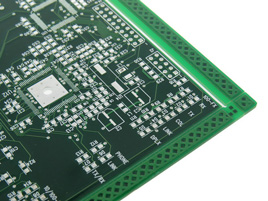
PCB Made in China
Advantages of conventional PCB
- Simple Via models.
- Low Cost (until layers count comes too high).
- Simple dielectrics—Primarily FR4.
- High reliability (until layer count becomes too high).
- Mature process, everybody does it. eg. 4 layers pcb, 6 layers pcb manufacturers in China. But the HDI circuit board is difficult, for the majority of Chinese PCB manufacturing factory. We have a HDI PCB plant – Changsha, China PCB factory – HDI PCB Production Quantities.
Disadvantages of conventional PCB
- Fewer China PCB manufacturers can obtain good yields, costs skyrocket.
- Via has to be large, reducing route-ability, increasing layers.
- Difficult to implement for BGA pin-pitches below 0.25mm.
- Through hole vias capacitively couple to every plane layer and signal losses increase with thickness.
- Long via stubs create impedance mismatches, reflections on single-ended nets.
- Large via pads often force diff pairs to be split under BGAs.
Conventional PCB Capabilities:
| Item | Technical Specification — Conventional PCB | |
| Conventional Rigid PCB | Strandard | Advanced |
| Layer up to | 16 Layers | 60 Layers |
| Base Laminate Type | CEM1 CEM3 | CEM1 CEM3 |
| FR4 High TG Aluminum | FR4 High TG Aluminum | |
| Board Thickness | 0.008″ / 0.126″ | 0.008″ / up to .325” |
| Min.Trace Width/Space | 0.075/0.075mm(3/3mil) | 0.05/0.05mm(2/2mil) |
| Outer layer copper thickness | Base copper 3OZ | Base copper 5OZ |
| Finish copper 4OZ | Finish copper 6OZ | |
| Inner layer copper thickness | 3OZ | 3OZ |
| Mini Hole Size | 0.25mm(Mechanical)/0.1mm(Laser) | 0.20mm(Mechanical)/0.1mm(Laser) |
| Aspect Ratio | 6:1 | 10:1 |
| Solder Mask Color | Red, Black, White, Yellow, Bule, Green | Red, Black, White, Yellow, Bule, Green |
| Impedance Control Tolerance | 7% | 5% |
| Surface Treatment | Immersion Ag | Immersion Ag |
| Immersion Gold | Immersion Gold | |
| Hasl | Hasl | |
| Lead Free Hasl | Lead Free Hasl | |
| Immersion Tin | Immersion Tin | |
| Flash Gold | Flash Gold | |
| ENIG+OSP | ENIG+OSP | |
| Hard Gold(10-30u”) | Hard Gold(10-30u”) | |
| Carbon | Carbon | |
| CNC V-Cut, Degree | 30, 45, 60 | 30, 45, 60 |
| V-cut by hand, Degree | 30, 45, 60 | 30, 45, 60 |
| Outline Profile | POUNCH and CNC | POUNCH and CNC |
| The angle type of the chamfer | 10-90 | 10-90 |
| Min./Max size can be plugged | 0.25/0.50mm | 0.25/0.65mm |
| Min.annular ring can be kept | 0.15mm | 0.13mm |
| Min.SM bridge for green SM | 0.1mm | 0.075mm |
| Tolereance of dimension Size | +/- 0.13mm | +/- 0.10mm |
| Tolereance of board thickness | +/- 10% | +/- 8% |
| Tolerance of the PTH | +/- 0.075mm | +/- 0.075mm |
| Automatic Board, Contersink holes and other depends on speical request. eg. gold finger pcb our factory accept.if your want turnkey printed circuit board original from China please choose Asia Pacific Circuits. | ||